
Nexstrom raises $12M to replace silicon with 2D semiconductor wafers
Singapore-based startup Nexstrom Pte. Ltd. has secured $12 million in seed funding to advance its wafer-scale platform for 2D semiconductor materials. The funding, led by Xora Innovation, aims to accelerate the commercialization of 12-inch 2D wafers designed to replace silicon in chipmaking, addressing critical inefficiencies in power consumption and performance.
LazyFounders
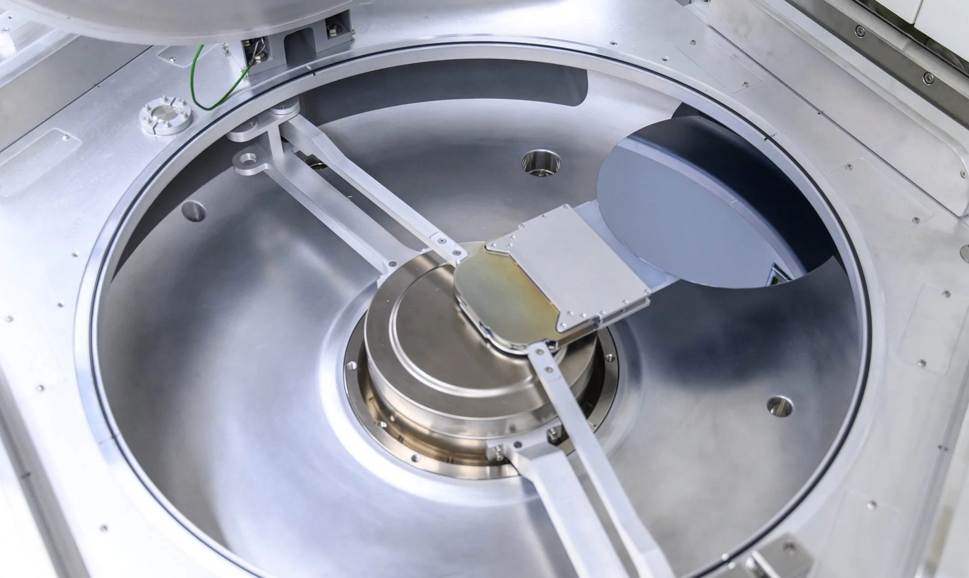

Singapore-based startup Nexstrom Pte. Ltd. has secured $12 million in seed funding to advance its wafer-scale platform for 2D semiconductor materials. The funding, led by Xora Innovation, aims to accelerate the commercialization of 12-inch 2D wafers designed to replace silicon in chipmaking, addressing critical inefficiencies in power consumption and performance.
30 SEC SUMMARY
- Singapore-based startup Nexstrom has raised $12 million in seed funding to advance its wafer-scale platform for 2D semiconductor materials.
- The funding round was led by Xora Innovation, with participation from SEEDS and Foothill Ventures.
- Nexstrom aims to replace silicon in chipmaking with 12-inch 2D semiconductor wafers, enabling more efficient and powerful chips.
- 2D materials reduce power loss and eliminate interface flaws compared to traditional silicon.
- The technology is designed to integrate with existing foundry workflows for scalable production.
TABLE OF CONTENTS
- Seed funding to advance 2D semiconductor wafers
- Why 2D materials could replace silicon
- Scaling production for the post-silicon era
- What this means
- Key takeaways
- FAQ
- Sources
KEY HIGHLIGHTS
- Nexstrom raises $12 million in seed funding, led by Xora Innovation.
- The startup aims to mass-produce 12-inch 2D semiconductor wafers to replace silicon.
- 2D materials reduce power loss and improve efficiency compared to traditional silicon.
- Nexstrom’s platform integrates with existing foundry processes for scalable production.
- The technology is already on the roadmaps of major semiconductor firms.
Seed funding to advance 2D semiconductor wafers
Nexstrom Pte. Ltd., a Singapore-based startup, has raised $12 million in seed funding to commercialize its wafer-scale platform for 2D semiconductor materials. The round was led by Xora Innovation, with participation from SEEDS and Foothill Ventures, according to SiliconANGLE. This brings Nexstrom’s total funding to $15 million.
The startup aims to replace traditional silicon in chipmaking with 12-inch 2D semiconductor wafers. These materials are designed to enable more efficient computing and reduce power loss, addressing key limitations of silicon-based chips.
Why 2D materials could replace silicon
Silicon’s physical limitations have become a bottleneck in chipmaking, particularly as demand for more powerful and energy-efficient chips grows, driven by advancements in artificial intelligence. According to SiliconANGLE, further shrinking silicon channels leads to electron leakage, resulting in power loss and inefficient computing.
Nexstrom is betting on single-crystal 2D substrates made from transition metal dichalcogenide materials as a solution. These materials eliminate interface flaws like 'micro-voids,' which contribute to electrical current leakage, making them a promising alternative to silicon.
Scaling production for the post-silicon era
Nexstrom claims to have developed the first platform capable of growing single-crystal 2D semiconductor materials at commercial scale. The company combines proprietary chemical vapor deposition hardware with a novel process technology to enable continuous growth of 12-inch wafers, according to SiliconANGLE.
The platform is designed to integrate with existing foundry workflows, which could lower the barrier to adoption for semiconductor manufacturers. This approach positions Nexstrom to meet the growing demand for advanced chips in AI and other high-performance applications.
SiliconANGLE reports that 2D semiconductor materials are already on the roadmaps of the world’s largest semiconductor firms, indicating industry-wide interest in this technology.
What this means
LazyFounders analysis — our interpretation, not reported fact.
Nexstrom’s seed round signals growing investor confidence in post-silicon semiconductor materials. For founders and operators in the chipmaking space, this is a reminder that the industry’s next frontier isn’t just about shrinking silicon further—it’s about fundamentally new materials that can address silicon’s physical limitations.
The ability to integrate 2D materials into existing foundry processes is a critical advantage, as it reduces the friction for adoption. If Nexstrom delivers on its promise of wafer-scale production, it could accelerate the transition to a post-silicon era, particularly for AI and high-performance computing applications where power efficiency is a bottleneck.
However, the challenge remains in scaling production while maintaining quality and cost competitiveness. Startups and incumbents alike will be watching closely to see if Nexstrom can turn this funding into a viable, mass-producible alternative to silicon.
Key takeaways
- Nexstrom has secured $12 million in seed funding, bringing its total raised to $15 million.
- The round was led by Xora Innovation, with SEEDS and Foothill Ventures participating.
- Nexstrom’s technology focuses on 12-inch 2D semiconductor wafers to replace silicon in chipmaking.
- 2D materials offer better efficiency and lower power loss compared to silicon.
- The company’s platform is designed to integrate with existing foundry workflows for scalable production.
- Major semiconductor firms are already exploring 2D materials, indicating industry-wide potential.
FAQ
What is Nexstrom’s technology?
Nexstrom is developing a platform to produce 12-inch 2D semiconductor wafers using single-crystal materials. These wafers are intended to replace silicon in chipmaking, offering better efficiency and lower power loss.
Why are 2D materials better than silicon for chips?
2D materials eliminate interface flaws like 'micro-voids,' which cause electrical current leakage in silicon. This reduces power loss and improves computing efficiency, making them a promising alternative for next-generation chips.
How does Nexstrom’s platform integrate with existing chipmaking processes?
Nexstrom’s platform is designed to work with existing foundry workflows, allowing semiconductor manufacturers to adopt 2D materials without overhauling their current production lines.
Who are Nexstrom’s investors?
The $12 million seed round was led by Xora Innovation, with participation from SEEDS and Foothill Ventures.
What is the potential impact of Nexstrom’s technology?
If successful, Nexstrom’s technology could accelerate the transition to a post-silicon era in chipmaking, particularly for AI and high-performance computing applications where power efficiency is critical.
Related on LazyFounders
Sources
- SiliconANGLE · 2026-09-22
Nexstrom bags $12M to help chipmakers replace silicon with more efficient semiconductor wafers
This story is an original summary and analysis written by LazyFounders from the reporting listed above. Facts are attributed to their original publishers; sections marked as analysis are LazyFounders's opinion. Where a source is in another language, facts were machine-translated and quotations are reported, not reproduced. Read the original coverage via the links.